Valencia, Spain, and Vaassen, The Netherlands (Sept 9, 2022) – UPVfab, the microfabrication facility at the Universitat Politècnica de València, has upgraded the low-pressure chemical vapor deposition (LPCVD) furnace on its system TS81003 manufactured by Tempress, to expand the portfolio of silicon nitride deposition, that now encompasses both stochiometric and low-stress silicon nitride. The upgrade was funded by the regional government Generalitat Valenciana through project GVA/IDIFEDER/2021/046 “Multi-level Microfabrication Technologies (T-MFAB-MN)” as part of a strategy to equip the facility for micro-fabrication in the technical disciplines of photonics, electronics, and chemical engineering.
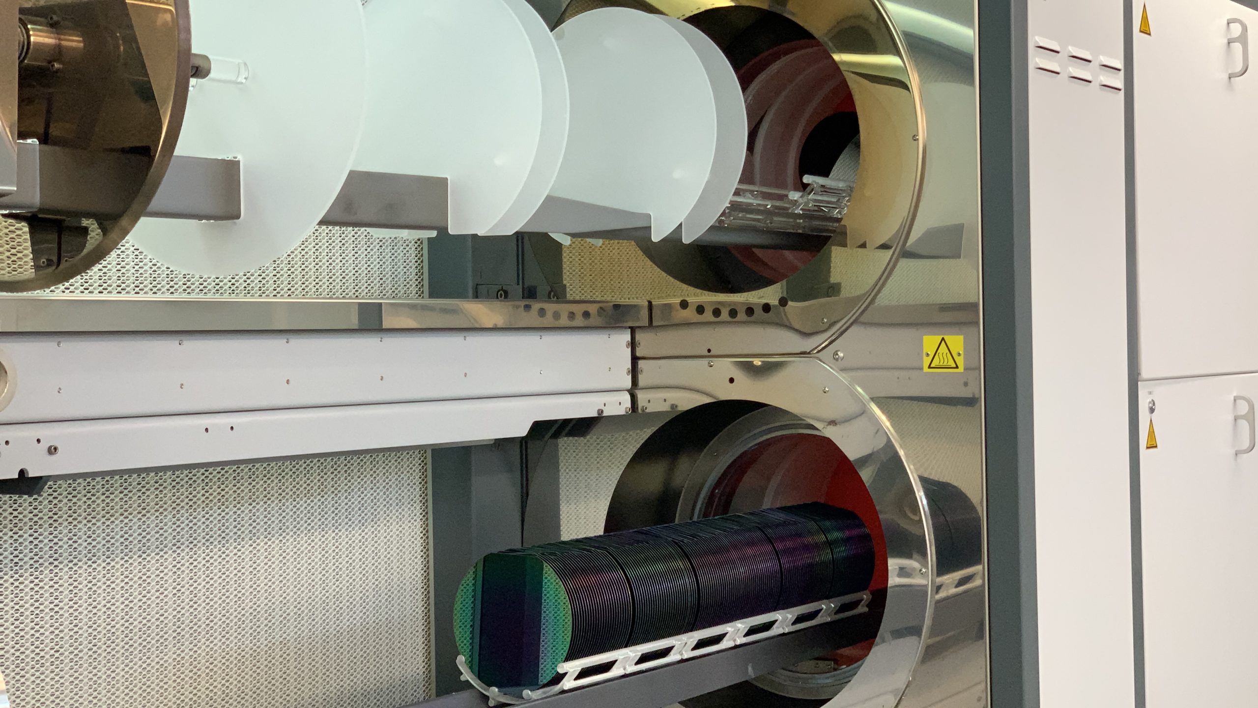
Tempress TS81003 system allows for very precise gas flow, temperature and pressure control, which leads to highly tunable material properties such as uniformity and stress levels of the silicon nitride layers. “We qualified the low stress silicon nitride process at UPVfab with 6 inch wafers”, Rob de Jong, Account Manager at Tempress shared. “The system can work with many types of wafers up to 8 inch, and as such is unique in Spain”.
“The Tempress TS81003 system is one of our flagship equipment, with three tubes including automation and process control monitoring, one for thermal processing (wet/dry oxidation of silicon and sintering), other for deposition of silicon nitride and the third to be upgraded in short for new processes,” said Dr. Gloria Micó, Facility Manager for UPVfab. “Our vision is industrial users find at UPVfab the right environment for micro-fabrication, where deposition complementary tools to the Tempress furnace, that provide plasma-enhanced CVD (PECVD) and sputtering systems, as well as lithography tools (mask and mask-less based) up to 8 inch wafers, and wet and dry etching equipment”. UPVfab established a resident company program in 2021. “The programme builds upon our infrastructure automation and personnel, that are ready to support industrial R&D, prototyping, and small series manufacturing, besides the establishment of demo sites in the cleanroom,” said Prof. Pascual Muñoz, Director for UPVfab.
About UPVfab
UPVfab is the micro-fabrication R&D and pilot line facility at Universitat Politècnica de València. The facility comprises 500m2 cleanrooms ISO-7 (class 10.000) and positions to serve with automation tools for backend processing of semiconductor wafers.
About Tempress
Tempress’ purpose is to support customers in the semiconductors, power, MEMS, photonics, solar, life sciences and coating markets to produce advanced materials and devices with high added value innovative furnace solutions. Tempress’ over 50 years of heritage in developing and producing diffusion and deposition equipment and related processes is a testament to the company’s flexibility, innovation, quality, and dedication.
Tempress’ technologies and products have advanced the semiconductor industry and we have installed more than 30 GW production capacity in diffusion furnace systems for solar panel production. Tempress’ headquarters is located in Vaassen, The Netherlands. Customers are supported throughout the world by its highly professional direct sales and service people and commercial partner network.
For more information, contact:
UPVfab
Dr. Gloria Micó
Facility Manager, UPVfab Microfabrication Facility,
Universitat Politècnica de València
+34.963.879.760
gloria.mico@upv.es
https://www.fab.upv.es/
Tempress
Mr. Rob de Jong
Account Manager
+31 622664580
rdejong@tempress.nl
https://www.tempress.nl